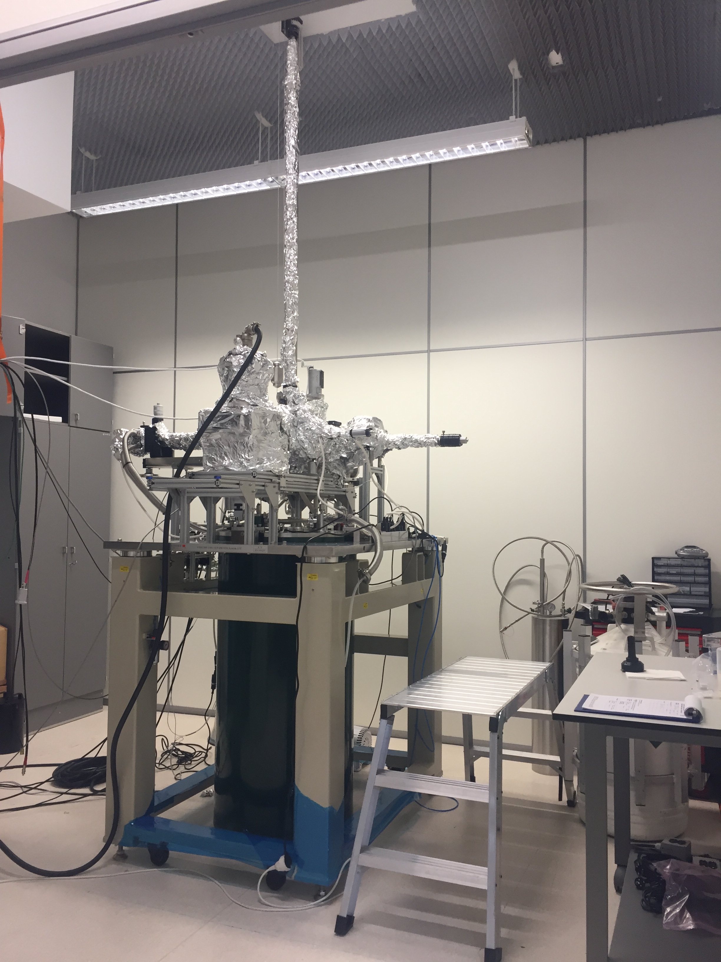
“Selenita” Molecular beam epitaxy (MBE) facility -This is our home-made MBE system for the growth of Se-based 2D materials and van der Waals heterostructures. It is equipped with four independent evaporators that provide large versatility during the growth, thus enabling the synthesis of estoichiometrically complex 2D materials and heterostructures.
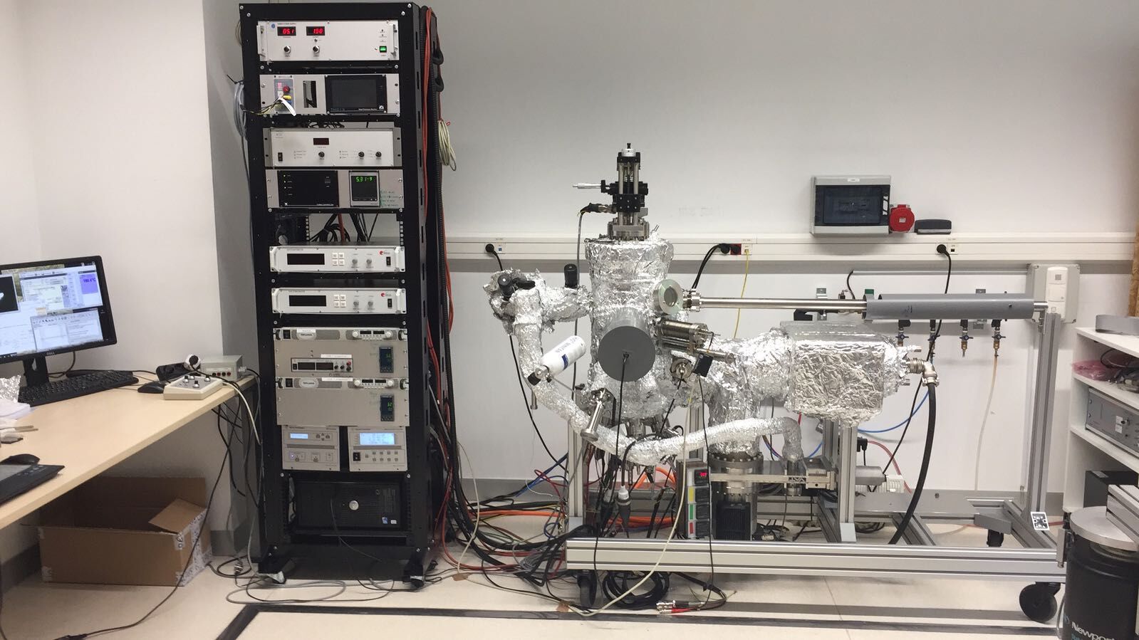
“Victoria” Unisoku 1300 Low Temperature (340mK) STM/transport system with 11T magnet and electron transport capability. – This system is our main tool for the structural and electronic characterization of epitaxial 2D materials and heterostructures.
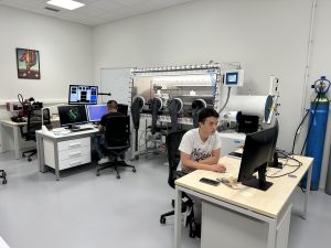 Nanofabrication laboratory facility -Here we stack our 2D-materials based heterostructures, including twisted moiré materials. The transfer stage and AFM capabilities are located inside an Argon glovebox to enable the fabrication of devices based on air-sensitive 2D materials. This space also includes plasma etching, optical microscopy, wire bonder, and UHV chamber for cleaning and deposition, etc.
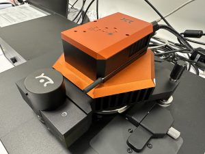
“Licancabur I” and «Licancabur II» «Ambient Atomic Force Microscopes (AFMs): Our ambient AFM systems enable the fast characterization of the morphology of our MBE-grown samples as well as nanofabricated moiré heterostructures. Furthermore, this system is used to probe the mechanical, electric and magnetic properties of our 2D materials using Kelvin probe microscopy, magnetic force microscopy, etc.
“Minerva» Unisoku 1600 Ultra Low Temperature (30mK) STM/transport system with 9T/2T/2T vector magnet and electron transport capability. – This system has been recently purchased to carry out the electronic characterization of moiré quantum materials. Installation scheduled by April 2025.