Our research interests lie in exploring the most fundamental properties of novel 2D materials and related heterostructures. Our efforts are summarized in the following three interconnected research lines:
Electron correlated 2D materials
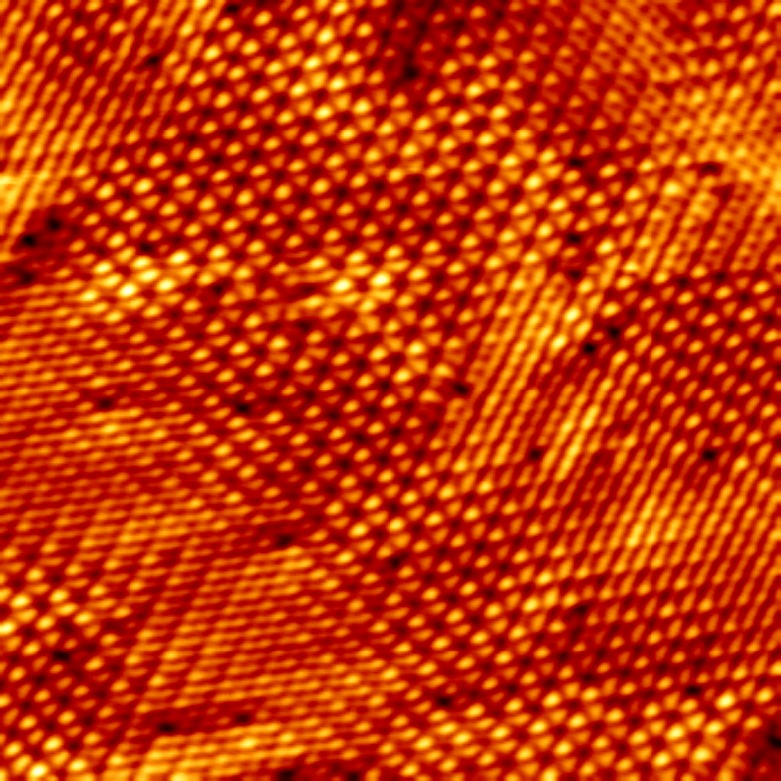 Novel 2D materials are subject to effects of reduced dimensionality when thinned down from bulk to the single-layer limit, which often impact their fundamental properties and overall response. We investigate these dimensionality effects mostly in few- and single layers of strongly correlated materials – transition metal dichalcogenides (TMD) as well as other classes of 2D materials – that exhibit collective electronic phases such as superconductivity, charge/spin density waves and the quantum spin Hall effect. Our group’s research approach is to combine sub-nm scanned probe techniques with mesoscopic electronic transport (see lab facilities) in order to build connections between fundamental physical properties of 2D materials at different length scales.
Manipulation of collective electronic phases
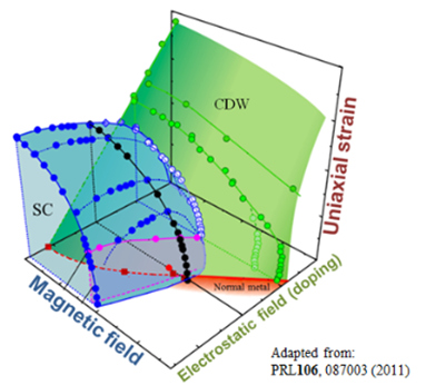
The main objective of this project is to demonstrate control over the electronic ground states of highly correlated 2D materials via external actuation such as the use of electromagnetic fields in order to build links of applicability for signal processing in electromechanical nanodevices. 2D correlated materials exhibit collective electronic phases such as superconductivity, which respond dramatically to external perturbations. The project aims to understand the interplay between these external stimuli and microscopic electronic phases, and to unambiguously correlate them with mesoscopic electrical transport and mechanical response.
Growth of van der Waals heterostructures
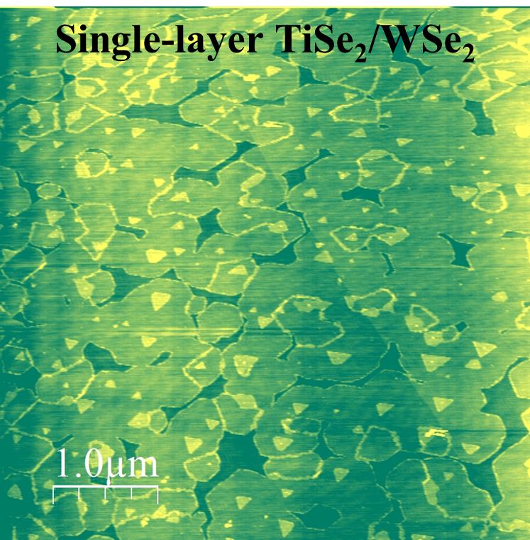
The growth of 2D correlated materials and related van der Waals heterostructures is of crucial importance for our research. It all starts here. Thin films of 2D correlated materials often degrade rapidly in ambient conditions compared to, for example, graphene. Therefore, molecular beam epitaxy (MBE) in ultra-high-vacuum conditions provides an ideal platform for the cm-scale growth of these materials. In our MBE lab we design and synthesize (see lab facilities) the layer/s of interest by investigating the micron- and nanometer-scale their morphological properties as a function of key parameters such as the substrate temperature, flux ratio and growth rate. This provides full understanding of the growth kinetics and morphology and enables the optimization of the crystal quality in terms of the domain size, density of defect, etc.